
The development of ARINC429 bus interface board realizes the reception and transmission of multi-channel ARINC429 bus data, which has become the focus of research on aircraft airborne bus interface.
1 Introduction to ARINC429 bus
On modern civil aircraft, a large amount of information needs to be transmitted between systems and systems, between systems and components. The ARINC specification is an industry standard for air transport developed to transmit digital data information between avionics.
The ARINC 429 (hereinafter referred to as 429) bus protocol was proposed by the Aviation Engineering Committee in July 1977 and was published and approved for use in the same year. Its full name is the digital information transmission system DITS. The protocol standard specifies the digital information transmission requirements between avionics and related systems. ARINC429 is widely used in advanced civil aviation aircraft, such as B-737, B-757, B-767, and Russian military aircraft have also adopted similar technology. Our corresponding standard is HB6096-SZ-01. The ARINC429 bus has a simple structure, stable performance and strong anti-interference. The biggest advantage is the high reliability, which is due to non-centralized control, reliable transmission, and good error isolation.
The 429 bus uses twisted-pair shielded cable to transmit information and is transmitted in reverse by a pair of twisted pairs. It has strong anti-interference ability. The modulation method adopts the three-state code method of bipolar return-to-zero system, that is, the three-level state modulation in which the information is composed of "high", "zero" and "low" states. The signal on the 429 cable and the level-converted signal are shown in Figure 1. Each word of the 429 bus is 32 bits, and its word synchronization is based on a time interval of at least 4 bits of the transmission period, that is, a 4-bit code word.
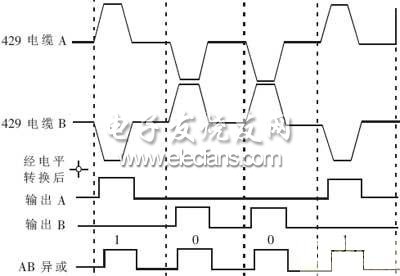
Figure 1 429 signal and level-converted waveform
2 system overall plan
The main function of the 429 bus interface board is to bridge the 429 signal and related peripherals. It can receive the 429 signal from the bipolar return-to-zero system and convert it into a digital signal for transmission to a computer or other device. Convert digital signals from a computer or other device to a 429 signal output. The bus interface board introduced in this paper uses FPGA and DSP to realize four 429 signal receiving channels and four 429 signal transmitting channels, and each channel is independent of each other. In this interface board, the time interval between every two data words is adjustable, and each transceiver channel can define the word interval length separately, and each channel check mode can be separately defined as odd parity or even parity, data transmission You can choose to send single frame or auto repeat (send a frame repeatedly).
The entire interface board consists of a modulation circuit, a demodulation circuit, an FPGA, a DSP, and a dual-port RAM, as shown in Figure 2.
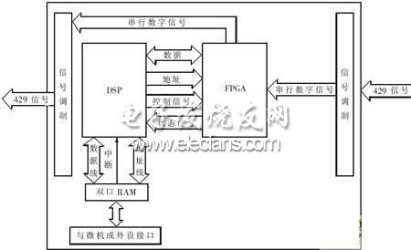
Figure 2 Interface board hardware structure
3 hardware circuit design
3.1 Modulation and demodulation circuit design
After the 429 signal enters the interface board, the 429 signal is first converted to a TTL level that the digital circuit can recognize. Here, HOLT's HI-8482 is used to demodulate the signal, converting the standard 429 bus signal into a 5V TTL digital signal. In order to reduce the interference, the four input pins of the 429 bus signal are respectively connected with 39pF high-precision military capacitors; the HOLT company's HI-8585 chip is used to realize signal modulation, and the TTL digital level is converted into the standard 429 signal.
3.2 FPGA internal logic design
According to the coding format, characteristics, transmission rules and protocol requirements of the 429 signal, an ALTERA company's ACEX1K type FPGA is used to transmit and receive four channels of data. Each way is divided into a receiving part and a transmitting part.
The main function of the receiving part is to convert the serial data into 32-bit parallel data by serial/parallel conversion, and automatically perform error control on the received data. Errors such as word interval and bit interval error can be automatically detected. If there is no error, the data is sent twice to the 16-bit data bus of the DSP for reading. The block diagram of the receiving module is shown in Figure 3.
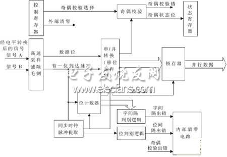
Figure 3 Receiver block structure block diagram
Shenzhenshi Zhenhuan Electronic Co Ltd , https://www.szzhpower.com