For hardware encryption, you must consider the problem of the computer interface. There are many types of interfaces for computers, such as traditional serial ports and parallel ports. The serial port appears in the 1980s, the data transmission rate is 115 ~ 230kb / s, generally used to connect the mouse and external Modem; the data transmission rate of the parallel port is 8 times faster than the serial port, the data transmission rate of the standard parallel port is IMb / s Left and right, generally used to connect printers, scanners, etc. The early software dog encryption hardware was basically using parallel port, which is not only easy to conflict with the printer, but also easy to be cracked. In order to design a more reliable and complete encryption hardware, a new computer interface must be adopted. In recent years, the development of fast USB interface technology has provided a good path for hardware encryption.
1 Proposal of the overall plan
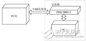
The design system principle is based on the principles of practicality, reliability, and economy, ensuring that the system not only meets the application needs, but also has flexibility, scalability, and versatility. The system is composed of EDA technology, USB bus protocol and encryption algorithm optimization. The structure of the system is shown in Figure 1. One of the functions of the FPGA is to communicate with the PDIUSBD12 to implement the USB protocol, obtain data from the PDIUSBD12, and send data according to the requirements of the host. The second function is the implementation of the encryption algorithm to complete the encryption of the transmitted data.
2 USB protocol implementation
2.1 Introduction to PDIUSBD12
PDIUSBD12 is a newer dedicated USB communication control chip from Philips. It conforms to the USBI.1 specification and is a high-performance USB interface device that integrates SIE, FIFO memory, transceiver and voltage regulator. High-speed parallel interface (2 MB/5) with any external microcontroller/microprocessor, IMB/5 data transfer rate and fully autonomous direct memory access DMA operation in both batch mode and synchronous mode.
2.2 USB controller design
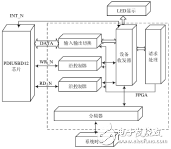
From the perspective of hardware implementation, the PDIUSBD12 controller is divided into a frequency divider module, a controller module, an input/output switching module, a device transceiver module, and a request processing module. After the structural design of the system is determined, the design of each module must first use the hardware description language (VHDL) to complete the description of the system, and then use the language level system simulation and debugging tools for language level function simulation and debugging.
The system is described in the VHDL language. The VHDL language is a structured language that supports structured design. Structured design is to divide a system into multiple sub-modules, and each sub-module can continue to be divided into more modules. Firstly, according to the functional description of the system, the system is divided into subsystems with clear interfaces and simple mutual relations, so as to obtain a system-level description. After that, the structural design and description of each subsystem (or functional module) is performed in turn. Refine step by step and finally complete the design. This actually gives a way to partition the module. When the system is divided, it is not that the modules of the system are divided into very detailed ones at a time, but are gradually refined from top to bottom according to the hierarchical thought. Figure 2 depicts the hardware block diagram of the processor. The functions of each module are defined as follows:
(1) Divider module
Since the PDUSBD12 has a time limit on the read/write timing, for example, the interval between each operation cannot be less than 50 ns, and the system clock frequency of the FPGA is generally high, so the system clock can not be directly used to control the PDIUSB12, and the frequency division must be performed. The function of the divider module is to generate a clock signal of the desired frequency as required by the system clock.
(2) along the controller module
The read and write operations of PDIUSBD12 each have a read/write control signal WR-N and RD-N. Each read and write operation is triggered on the falling edge of the corresponding control signal. The function along the control module is controllable to generate a falling edge. Signal for controlling read and write operations.
(3) Input/output switching module
The input/output switching module is very important in the whole system, because the data bus between the FPGA chip and the PDIUSBD12 chip is a bidirectional bus, so when one of the read and write operations is in progress, the source of the other operation must be turned off, otherwise Will cause double drive, which will not only get the correct data but also damage the chip. The function of the input/output switching module is to control the signal source according to the current read and write status, ensuring that only one signal source drives the bus at a time.
(4) device transceiver module
This module is the core module of the entire firmware. His work includes configuring the PDIUSBD12 chip, processing the interrupt generated by the PDIUSBD12, completing the reading of data from the cache, and sending the data through the PDIUSBD12 as needed. The device transceiver module completes the parsing of each host request, and in addition, passes the parsed request data to the request processing module.
(5) Request processing module
The role of the request processing module is to receive a host request that the device transceiver module parses and decides how to handle the request.
3 implementation of encryption algorithm
3.1 Advantages of hardware encryption
With the development of the information industry, the integrated circuit industry provides more and more powerful chips. Now all encryption products are in specific hardware encryption form. These encryption/decryption chips are embedded in the communication line and then encrypt all the passed data. While software encryption has become popular today, hardware is still the primary choice for commercial and military applications.
(1) speed
Encryption algorithms usually contain many complex operations on plaintext bits. No such type of operation can be performed on a general computer. Two of the most commonly used encryption algorithms, DES and RSA, are not efficient at running on general purpose microprocessors. In addition, encryption is often a high-intensity computing task. Computer microprocessors are not efficient, and the encryption is moved to the chip, which can share the work of the computer microprocessor and speed up the entire system.
(2) Security
For each encryption algorithm running on a general computer without physical protection, it is likely that someone with ulterior motives will use various tracking tool password modification algorithms to make it unknown to anyone. Hardware encryption devices can be securely packaged to avoid such things, and tamper-proof boxes can prevent others from modifying hardware encryption devices. Special purpose VLSI chips can be covered with a layer of chemicals, so any attempt to access them internally will result in the destruction of chip logic.
(3) Easy to install
Most encryption applications are not related to ordinary computers, and it is much cheaper to place dedicated encryption hardware in phones, fax machines, and modems than in microprocessors or software. Even when the encrypted data comes from a computer, it is easier to install a dedicated encryption device than to modify the computer system software. Encryption should be invisible and should not interfere with the user. The only way for the software to do this is to write the encryption program at the bottom of the operating system software, which is not easy.
3.2DES encryption algorithm implementation
The DES (DataEncrypTIonstandard) encryption algorithm has experienced a long-term test as it has become an encryption standard. Practice has proved that the security of the DES algorithm is able to meet most of the security requirements. The DES algorithm implemented by software will occupy system resources to a large extent, causing serious degradation of system performance. The DES algorithm itself does not have a lot of complicated mathematical calculations, and only logic in the encryption/decryption process and key generation process. Operation and table lookup operations, therefore, hardware implementation is an ideal solution from the perspective of system performance or encryption/decryption speed.
The key part of the DES algorithm design is the design of 5 boxes, the generation of each round of keys and the pipeline design during the entire 16-round encryption process.
According to the actual needs, the encryption algorithm module is designed independently, as shown in Figure 3 is the schematic diagram of the encapsulated I/0 interface.
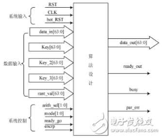
As the input interface includes 3 major parts, system input, data input and system control. The system input is mainly the clock signal input ClK and the system automatic restart signal RST when an abnormal situation occurs. The clock signal input can use the system clock of the encryption board or use its own clock independently.
Here, in order to facilitate expansion and upgrade, a jumper is used to select a clock signal, and two clock frequency selections are supported.
The data input part includes 64-bit encrypted data input data_in[63:o], 64-bit key input key1[65:o], key2[63:0], key3[63:0] and initialization vector rant Val[63:0]. Since the USB bus interface is a serial bus, the encrypted data sent from the master device must be saved by the latch before entering the encryption chip. Similarly, as the key data, the latch is also required to be saved to ensure the input data. Integrity. The output interface mainly includes 64-bit encrypted data output dat_out[63:0], output ready signal ready-out, system busy signal, busy and error feedback signal par-err. After the system completes the encryption of the data, it will promptly notify the ready_out signal to rise from the low level to the high level, and the busy signal becomes active low, so that the post module will judge whether the output should be read according to the ready_out and busy signals. data.
(1) implementation of the s box
The s box is a key to the DES algorithm, because there are 8 s boxes in each round of calculations, and a total of 16 rounds of encryption, a total of 128 s boxes are required, so the implementation efficiency of the s box is particularly important. The s box is a complex nonlinear function. When the hardware is implemented, the implementation of the s box has certain difficulty. The quality of the design is the main factor affecting the overall encryption and decryption speed of the algorithm. In the design, from the resource point of view, the consumption of logic unit (LE) and embedded array block (EAB) in FPGA devices should be minimized, but this may be at the cost of reducing system speed. From a speed point of view, the system processing speed should be maximized, but this often requires more resources. Therefore, in most cases these two options are contradictory and need to be weighed according to the actual environment.
Therefore, the principle followed in this paper is to save resources as much as possible while ensuring speed. This design uses the case statement in the VHDL language to directly implement the nonlinear transformation of the s box.
(2) Implementation of the key generation unit
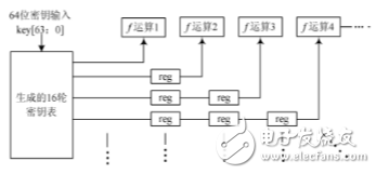
The key generation unit is constituted by a selection control circuit PC_1, a cyclic shift register, and a compression permutation circuit PC-2. The input to this part is the 64 b initial key; the output is the subkey used for each iteration. For a total of 16 rounds of loop operations, each round of key usage is used in the same manner as shown in Figure 4. In the first cycle of the initial key input, all the different keys required for 16 rounds of encryption are simultaneously output in parallel, and then In the corresponding cycle order, each round of key output is delayed by one clock cycle using the register as the key input of the round algorithm.
The advantage of this method is that each round of the key will be prepared before each round of operation, which is convenient for the encryption process. The design of this paper is to generate all the 16 rounds of keys through the multiplexer at one time, similar to the generation of a "key pool", and then the different rounds are sequentially saved by the registers and synchronized with the pipeline. Here, when the key is generated, since the order of decryption and encryption is reversed, the right shift is generated at the time of decryption.
(3) Implementation of the pipeline
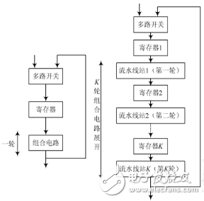
Pipelining is a common way to increase the amount of data processed by a digital circuit per unit of time. His concept is to divide the logic operations performed in one clock cycle into smaller operations and complete them in multiple higher-speed clocks, such as Figure 5 shows.
In this configuration, the combinational logic corresponding to the K-round encryption is equally divided into K parts, and an additional register is added between the respective parts, and the remaining components are the same as the basic structure. The portion of the combined logic circuit resulting from these partitions is called a pipeline station, and each pipeline station performs different processing steps. In this way, the circuit can process multiple blocks of data at the same time, increasing the amount of data that the system processes in a unit of time, that is, speed.
At each clock cycle, the partially processed data block is moved to the next pipeline station, and the subsequent block is immediately followed, occupying its original position, that is, a pipeline circuit can simultaneously encrypt and contain the pipeline station it contains. An equal number of data blocks. With this processing method of expanding the loop into a pipeline, the expanded pipeline processing cycle is ideally close to 1/K of the basic structure processing cycle time.
The DES algorithm implemented in this paper has a simple data flow path, most of which is a linear transformation for bits; the core part of the algorithm is 16 rounds of identical linear transformation iterations, so it can be looped into a 16-level pipeline; in non-feedback mode When applied, there is no correlation between the data blocks before and after, so there is no conflict; the subkeys needed in each round of operations can be generated in advance, and are provided to the pipelines as the data stream advances in the pipeline.
4 Conclusion
The design idea of ​​combining USB bus technology with EDA technology makes the system design more flexible and system upgrade easier. The generalization of the software platform, the standardization of the software protocol, and the unification of the hardware structure are realized, thereby ensuring the portability and scalability of the system, and providing a new idea for the design of the hardware encryption system. The actual operation of the encryption system shows that the system design idea is correct, and the system real-time and encryption performance can meet the design requirements.
Wireless Barcode Scanner,Bluetooth Barcode Scanner,Wifi Barcode Scanner,Portable Barcode Scanner
ShengXiaoBang(GZ) Material Union Technology Co.Ltd , https://www.sxbgz.com
