
Adaptability to network topology changes
The different configuration of the network determines its ability to adapt to changes in the network topology, which depends on whether a dynamic routing protocol is used in the network.
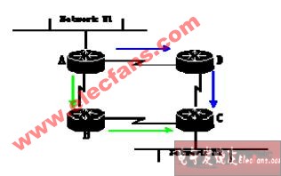
Static routing information can guide the normal forwarding of packets. In the network shown in the figure, in order to reach the target network N2, configure a static route on router A to point to router D, and configure a static route on router D to point to router C, so that packets sent from network N1 to N2 can be After reaching the destination network N2 through routers A, D, and C.
But if there is a problem with the path from Router A to D, Router A cannot send packets to Router D according to the static routing instructions. If you want to ensure the smoothness of the network, the network administrator must manually configure a static route through Router B, so that the message can pass through Routers A, B, and C, and finally reach the destination network.
If a certain dynamic routing protocol (such as RIP protocol) is running in the network, the situation will be different. When the route through Router D fails, the routing information between the routers will be transmitted through the dynamic routing protocol, and another route to the target network via Router B will be automatically discovered, and the routing table will be modified to guide the correct forwarding of the packets.
BGA PCB , it's the PCB that have the pads for BGA parts. BGAs (Ball Grid Arrays) are SMD components with connections on the bottom of the component. Each pin is provided with a solder ball. All connections are distributed in a uniform surface grid or matrix on the component. Common grids are nowadays: 1.27 mm - 1.00 mm - 0.80 mm - 0.50 mm.
PCB = printed circuit board and PCBA = printed circuit board assembly. For PCB, it means the copper circuits be printed on a board, and so the main composition of PCB are copper and board.
The copper is the circuits material and the circuits designed by the PCB designers. Depends on the current in the circuits, the PCB copper thickness could be done with 0.5oz-10oz. But the PCB designers need be noted that the copper track width/space need be enlarged with the thickness. For example, the minimum copper track width/space could be 3mil/3mil with 0.5oz, but would be 4mil/4mil with 1oz.
The PCB board could be rigid PCB, could be flex PCB and also could be Flex-Rigid PCB. And the materials could be FR4, PI, Aluminum, Copper-based, Rogers, Teflon, etc. They have different applications. For example, FR4 PCB is the most commonly used for rigid PCB and almost good for all electronics products; PI is the most commonly used for flex PCB; Aluminum and copper-based have good thermal diffusivity and always used for LED PCB ; Rogers PCB and Teflon PCB are always used for High Frequency PCB, etc.
We are the one-stop shop for all kinds of PCB manufacture service from PCB Prototype to big volume, which could save our customers a lot of time and money.
PCB Manufacture Capabilities
|
Features |
Capabilities |
|
Layers |
1-36 layers |
|
Material |
FR-4, Aluminum, Copper, Polyimide, high frequency (Rogers, PTEE, PI), etc. |
|
PCB Type |
FR-4 Standard PCB , Aluminum PCB , Copper-based PCB, HDI PCB , Rigid-Flex PCB, Flex PCB, Thick Copper PCB and Rogers PCB, etc. |
|
Board Thickness |
0.1mm-6.0mm |
|
Copper Thickness |
1/2oz-6oz(18um-210um) |
|
Biggest Board size |
600mm*1200mm |
|
Min Tracing/Spacing |
0.075mm/0.075mm (3mil/3mil) |
|
Min drilling Hole diameter |
0.15mm(6mil), 0.1mm(4mil)-laser drill |
|
Solder Mask |
Green, Black, White, Red, Yellow, Blue and Purple, etc. |
|
Silkscreen color |
White, Blue, Black, Red, Yellow |
|
Surface finish |
HASL Lead free, Immersion Gold (ENIG), Immersion Tin, Immersion Silver, OSP, Carbon oil, etc. |
|
Special Techniques |
Impedance Control, Gold Fingers, Blind/Buried vias, Peelable solder mask, Half holes, Via-in-Pad and Countersink hole, etc. |
PCB Products Show

PCB Factory Show

BGA PCB
BGA PCB,BGA PCB Board,SMT BGA PCB,BGA PCB Support
ZhongFeng Electronic Technology Co., Limited , https://www.dopcba.com