
Test principle and application of power amplifier TDA7294
1. Chip description TDA7294 is a novel DMOS high-power integrated circuit that was launched by the famous European SGS-THOMSON STMicroelectronics in the 1990s to mainland China. It sweeps the sound, cold and hard sounds of the linear amplifier and thick film integration in the past, and is widely used in the field of HI-FI: such as home theaters and active speakers. tda7294.pdf
The design of the chip is focused on sound, and has the advantages of bipolar signal processing circuit and power MOS. It has the characteristics of high pressure resistance, low noise, low distortion, and affinity for replaying sound. It also has silent standby function, short circuit current and overheat protection function to improve its performance. The relevant electrical parameters are as follows.
Working voltage range: (VCC + VEE) = 80V
Output power: up to 100W
Voltage range: | VCC | + | VEE | = 20V-80V
Quiescent current: 30MA
Output power: | VCC | = | VEE | = 35V, RL = 8 ohm is 70W
Total harmonic distortion (THD): 0.01% (typical value)
Conversion rate (SR): 10V / us
Open loop gain: 80dB
The purchase price is 13 yuan per person at the author ’s location; due to limited conditions, the test circuit is soldered with a universal board, as long as the speaker is not too difficult. The sound quality is not bad; because the author ’s technology is not yet mature, to master the sound effects of this chip, please master Pointing improvements.
2. The function of each end of the pin data is as follows:
Pin 1 is the standby terminal; Pin 2 is the inverting input terminal;
Pin 3 is the positive phase input terminal; Pin 4 is grounded;
5, 11, 12 feet are empty feet; 6 feet are bootstrap ends;
Pin 7 is + Vs (signal processing part); Pin 8 is -Vs (signal processing part);
9 feet are standby feet; 10 feet are silent feet;
Pin 13 is + Vs (last stage); Pin 14 is the output terminal;
15 feet are -Vs (last level). 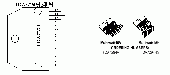
3. Description of circuit diagram R1, R2 and R5 form a typical power amplifier with an amplification factor of approximately 32 times that of R5 / R1;
2. C1, C2, C8, C9 are power supply filter capacitors;
3. Pin 9 and pin 10 can be added with switches to control standby and mute. C6 and C7 are used for filtering and debounce. 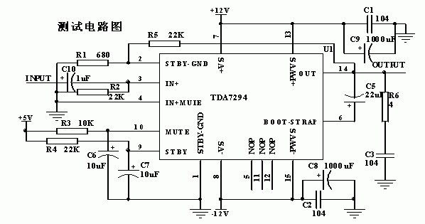
4. Test conditions 1. No load, use WD-5 voltage source + 12.1 -12.1 +5.0 to provide power and allowable bits.
2. Use SG1732SB5A DC stabilized current supply as input.
3. Use the multimeter SYG DT9205G to measure the value. 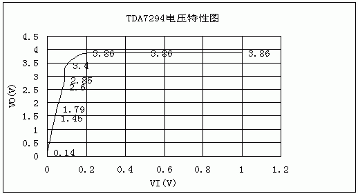
Fifth, the test summary started the test and mistakenly believed that the linear range was low. After analysis, the amplification factor was too large, but the maximum voltage of 3.86V was still too small to be suitable for certain high-voltage output requirements; it is still good as a general audio chip (excluding fever) .
Disclaimer: This article is Liang Weiwen's original work, if you need to reprint, please contact the author
Product application:
â– Products for commercial,household,lighting
Product features:
â– High strength,impact resistance and thermal stability
--Panel material using high quality polycarbonate
â– High resistance to deformation
---Long term use without obvious distortion
â– Flame retardant grade
----The flame retardant grade of panel is in line with UL94-V2
â– Adaptation property
----American Standard socket adapter all accord with NEMA
Standard
Colour: Black Brown White lvory Almond Gray Red
Wall Plate UL,Electrical Wall Plate UL,Wall Wall Plate UL,Double Duplex Outlet Wall Plate UL
Hoojet Electric Appliance Co.,Ltd , https://www.hoojetgfci.com