
The ADS8684 is a 4-channel integrated data acquisition system based on a 16-bit successive approximation (SAR) analog-to-digital converter (ADC). This section introduces the ADS8684 features, application range, reference design circuitry, and circuit analysis to help you reduce design time.
ADS8684 features:
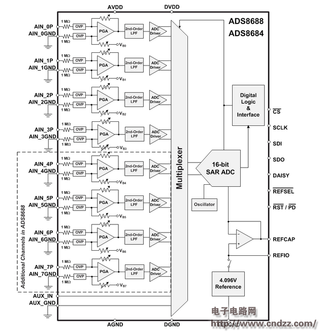
The ADS8684 provides an integrated analog front-end circuit for each input channel (overvoltage protection up to ±20V), a 4-channel multiplexer that supports both automatic and manual scan modes, and an on-chip 4.096V reference with low temperature drift. When powered from a single 5V analog supply, each input channel on the device supports both bipolar and unipolar inputs. The ADS8684 also provides a simple SPI-compatible serial interface for connecting to a digital host and supports daisy-chaining multiple devices.
Typical applications for the ADS8684 include: power automation, protection repeaters, PLC analog input modules
ADS8684 internal structure block diagram:
ADS8684 reference design circuit:
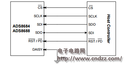
ADS8684 application circuit analysis: CS (Input): CS indicates an active-low, chip-select signal. CS is also used as a control signal to trigger a conversion on the falling edge. Each data frame begins with the falling edge of the CS The device input channel to be converted during a particular frame is selected in the previous frame. On the CS falling edge, the devices sample the input signal from the selected channel and a conversion is initiated using the internal clock. The next data frame can be input during this conversion process. When the CS signal is high, the ADC is considered to be in an idle state. SCLK (Input): This pin indicates the external clock input for the data interface. To the device are timed with respect to the falling edges of the SCLK signal. SDI (Input): SDI is the serial data input line. SDI is used by the host processor to program the internal device registers for device configuration. e Ach data frame, the CS signal goes low and the data on the SDI line are read by the device at every falling edge of the SCLK signal for the next 16 SCLK cycles. Any changes made to the device configuration in a particular data frame are applied SDO is used by the device to output conversion data. The size of the data output frame varies depending on the register setting. The SDO is used by the device to output conversion data. For the SDO format; A low level on CS releases the SDO pin from the Hi-Z state. SDO is kept low for the first 15 SCLK falling edges. The MSB of the output data stream is clocked out on SDO on the 16th SCLK falling Edge, followed by the subsequent data bits on every falling edge after. The SDO line goes low after the entire data frame is output and goes to a Hi-Z state when CS goes high.
ADS8684 Chinese information: Click to download
Popular application circuits with schematics and source code can be found at:
A power inverter, or inverter, is a power electronic device or circuitry that changes direct current (DC) to alternating current (AC).The resulting AC frequency obtained depends on the particular device employed. Inverters do the opposite of "converters" which were originally large electromechanical devices converting AC to DC.
Power Inverter kinds:
1.On grid inverter
2. Off grid inverter
Off Grid Hybrid Solar Inverter,Off Grid Power Inverter,Luminous On Grid Inverter,On Off Grid Hybrid Inverter
NANTONG RONGCHANG IMPORT&EXPORT CO.,LTD , https://www.ergsolarcn.com