
 At present, the experimental contents of the basic courses of digital electronic technology include three parts: confirmatory experiments, comprehensive experiments, and design experiments. The focus of each part of experimental content arrangement is different. For example, the design experiment is the key to design, require students to design a reasonable experimental circuit, and select the device, installation and debugging to complete the experimental content. From the teaching practice point of view, most students can successfully complete the experimental requirements, but the thinking of solving problems is single, the design process is not flexible, and the training of innovative thinking skills is not paid attention. This requires the teacher to arrange the experiment content at the same time, continue to guide students through a variety of ways to broaden their knowledge, innovative ways of thinking, treat the same problem, and actively explore a variety of ways to solve the problem. The combinational logic circuit design is various, I choose a kind of parity check circuit to carry on the detailed elaboration.
 The parity-check circuit has certain typicality and practicability in the analysis and design of the combinational logic circuit. Familiar with the logic function and circuit realization of the odd-odd circuit, it helps to deepen the understanding and mastering of the combinational logic circuit. Taking the example of odd circuit implementation as an example, various implementations of gate circuits, decoders, and data selectors are discussed, and the flexibility and diversity of combinational logic circuit design are illustrated with examples.
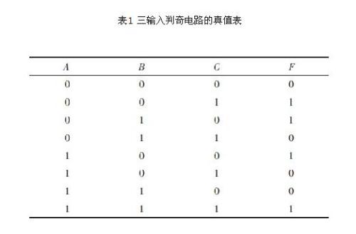
1 The truth table and expression of the three-input-variable-arbitrary circuit are used to determine the singularity of a three-input variable. Its input variables are denoted by A, B, and C respectively, and the output function is denoted by F. When there is an odd number of 1 in the value combination of the input variable, the output function value is 1; when the number of 1 in the input variable value combination is an even number, the output function value is 0, according to which the logic relationship can be written The truth table of the three-input variable arithmetic circuit is shown in Table 1.
As can be seen from the truth table 1, there are 4 groups of input variables that make the output function value 1 . Using an inverter, an AND gate, or a gate to realize a three-input odd circuit, its characteristic is that the expression basically does not change, and the realization way is simple and straightforward. The disadvantage is that there are many lines and the circuit is complicated.
Guangpu Electronics Co., Ltd , http://www.fjledlight.com