
In the traditional industrial control application, because the high-performance graphics card is integrated in the industrial control computer, the architecture of the industrial control computer + liquid crystal display is usually adopted, and the human-machine interface mainly composed of graphics and characters can be conveniently realized. In the aerospace field where real-time performance and reliability are relatively high, it is usually required to integrate a graphic display function inside the liquid crystal display to reduce the burden on the main control processor and improve the real-time performance of the system. This paper focuses on how to use FPGA to realize 2D graphics rendering based on Bresenham algorithm (including drawing points, drawing lines, drawing circles, drawing ellipses), as well as displaying dot matrix characters and bitmaps on the LCD screen, and proposing display performance optimization. A series of strategies. Through simulation verification and practical application of the product, the design method realizes stable and good performance of the graphic and character display functions of the liquid crystal display module, and is suitable for the application requirements of the high reliability liquid crystal display module in the aerospace field.
1 IntroductionIn the traditional industrial control application, the industrial control computer of X86 architecture is adopted, and the external VGA/DVI video signal is outputted by the computer external or integrated graphics card, and the display function is completed by the liquid crystal display. It is more convenient to implement human-machine interface by software programming under this architecture. In the field of embedded systems, especially in the field of information display of aerospace instrument display devices, the reliability and real-time requirements of display tasks are very high. On the one hand, it is necessary to reduce the modules and interconnection buses inside the device to improve the reliability of the device and reduce the power consumption; on the other hand, the high reliability processor selected by the device is usually low in performance, and requires a special hardware accelerator to assist the display function. . The hardware accelerator mainly performs functions such as character display, chart drawing and LCD screen driving to reduce the burden on the processor and improve the real-time processing of the external communication bus. FPGA-based liquid crystal display drivers and graphics accelerators are designed to meet display instrumentation. Since the graphics and display functions are integrated inside the liquid crystal display module, the performance requirements of the device host processor are greatly reduced, so that a low-performance, high-reliability processor can be used to perform display control tasks.
2 system structure2.1 Overall structure
The structure diagram of the instrument equipment system is shown in Figure 1. It consists of a data acquisition and communication host and a liquid crystal display module.
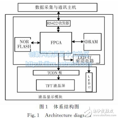
2.2 Data Acquisition and Communication Host
The data acquisition and communication host adopts 51 series single-chip microcomputers, external A/D acquisition, CAN and other interfaces, mainly completing data acquisition, communication and sending page display commands to the liquid crystal display module.
2.3 Interface
The LCD display module and the device host are RS422 serial interface, the communication baud rate is 200kbit/s, the data transmission protocol is customized, consisting of frame header, packet length, command, parameters, checksum, single data packet. The maximum length is 256 bytes.
Frame header: 0xEB, 0x90 two bytes, providing synchronization function for the communication process of the entire data frame;
Byte length: 1 byte, the total number of bytes of instructions in the data frame format, up to 255 bytes.
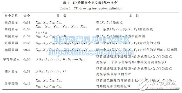
Instruction: The contents of the liquid crystal display module operation instructions, including commands and parameters. Table 1 gives the format and meaning of some operation instructions;
Checksum: 1 byte, the sum of the "byte length" and "instruction" fields to verify the correctness of the data frame.
2.4 LCD module
The liquid crystal display module is equivalent to a small liquid crystal display terminal, and is composed of a liquid crystal screen and its TCON board, backlight, graphic acceleration and display control board.
The drawing commands to be completed by the liquid crystal display module are: screen erasing (background fill), drawing points, drawing lines, drawing rectangles, drawing ovals, drawing circles, string display, custom word display, picture display, block copy, block paste And other functions, as well as font and image download functions. In addition, there are commands such as LCD brightness adjustment and status management.
The definition of 2D drawing instructions is shown in Table 1.
The LCD screen selected for this design is NEC's 16.5cm (6.5in) TFT color liquid crystal display with a resolution of 640 & TImes; 480, the LCD screen comes with TCON board, and its interface is 18bit digital RGB signal.
3 FPGA design implementationThe work done by the FPGA in this design is mainly: on the one hand, data reception and parsing, graphic drawing operation according to the command, generating display frame storage write operation data stream, and finally writing the data to be rewritten into the SDRAM memory; According to the timing requirement of the LCD synchronization signal, the data in the display area of ​​the frame memory is periodically read out to generate a liquid crystal screen driving data stream. Secondly, the FPGA also has a PWM signal generating module inside, which can adjust the brightness of the liquid crystal display.
3.1 FPGA device selection
The FPGA uses the Xilinx 2V3000 series [1], which has 28,672 LUT units and 28,672 flip-flops and 96 BlockRAMs for large-scale control logic and FIFO, Buffer, etc. In addition, the FPGA has DCM inside, which can The external 65MHz clock is converted to a 25MHz clock, which is used to drive the clock on the LCD screen, and can internally generate a 1kHz PWM signal by frequency division for LCD backlight brightness adjustment.
Fiber Optic Cabinet,Fiber Cabinet,Fiber Distribution Cabinet,Outdoor Fiber Cabinet
Cixi Dani Plastic Products Co.,Ltd , https://www.dani-fiber-optic.com