introduction
Electronic equipment usually uses a casing to shield the external electromagnetic field from interference. The outside of the casing usually opens holes to provide ventilation and visibility. Such openings allow external electromagnetic fields to be coupled to the inside of the equipment casing through the holes. Current and voltage are induced on equipment or printed circuit boards inside the enclosure, reducing the performance of the equipment or components and causing damage to internal equipment in severe cases. Therefore, it is of great practical significance and value to study the effective shielding effectiveness of electromagnetic shielding effectiveness of electromagnetic shielding. From the previous research, there are many ways to improve the shielding effectiveness. For example, under the same area, the shielding effectiveness of the hole array is better than that of the single hole. The shielding effectiveness of the double hole is better than the shielding performance of the single layer. The influence of factors on shielding effectiveness, such as hole size, shape, hole spacing, electromagnetic wave polarization direction, etc. This paper mainly deduces the shielding effectiveness formula of double-layer loading circuit board shielding cavity, and uses CST simulation to verify the influence of board size, position and quantity on the shielding effectiveness of the back cavity center point.
1 theory
The model of the shielding cavity in which the plane wave is vertically illuminating the double-layered rectangular hole-loaded circuit board is shown in Fig. 1. In general, the energy coupled into the shield cavity by the slot is greater than the energy entering the shield cavity through the cavity wall, so only the coupling energy is considered.
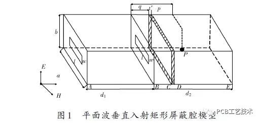
In this paper, a two-layer shield cavity model with copper is used, which is divided into two parts: the front cavity and the back cavity. a, b is the width and height of the shielding cavity, the length of the front cavity is d1, the length of the back cavity is d2; w, l is the length and width of the opening in the cavity; p is the central observation point of the back cavity; q is the inner layer The distance from the hole to the PCB; the thickness of the PCB is t'; the thickness of the cavity is t.
According to the transmission line theory proposed by MP Robinson, the hole joint is equivalent to a coplanar strip-shaped transmission line short-circuited at both ends, and the rectangular casing is equivalent to a short-circuited waveguide. The equivalent circuit diagram of the model is shown in Figure 2.
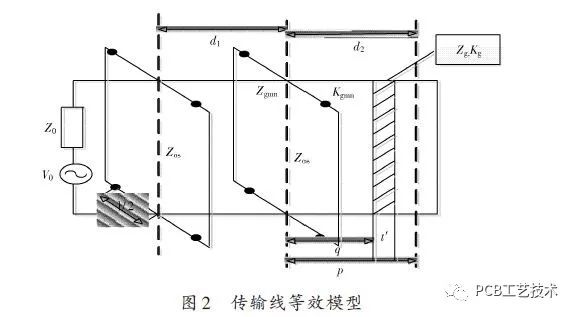
In Fig. 2, V0 is the equivalent radiation source, Z0 is the air wave impedance, about 377 Ω, Zos is the characteristic impedance of the hole slit, and the characteristic impedance and propagation constant of the equivalent rectangular waveguide are Zgmn and Kgmn.
The slotted characteristic impedance is derived from the formula [6] given by Gupta:
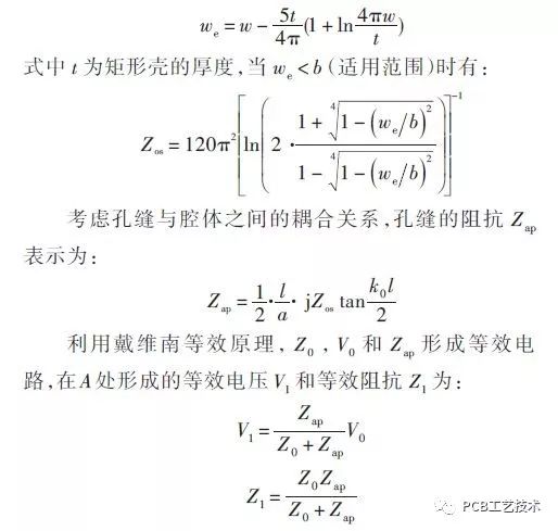
After the transmission line between AB, the equivalent voltage V2 and equivalent impedance Z2 of point B can be obtained by the Thevenin theorem:
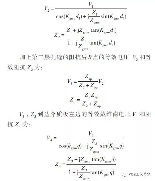
The board is a complex whole, which includes metal plates, wires, electronic components and lossy media. It is replaced by a macroscopic dielectric plate with a conductivity of σ = 0.22 S - m-1 and a dielectric constant of εr = 2.65. PCB [7-8], its characteristic impedance and propagation constant are Zg and Kg. When the size of the dielectric plate is infinitely close to the cross-section of the rectangular cavity, the reflection of the electromagnetic field in the cavity on the surface of the dielectric plate is negligible, which is obtained by the transmission line theory. The voltage at the left end of the dielectric plate is transmitted through the dielectric plate of thickness t' to the voltage V5 on the right side of the plate and the impedance Z5 is [6, 8]:
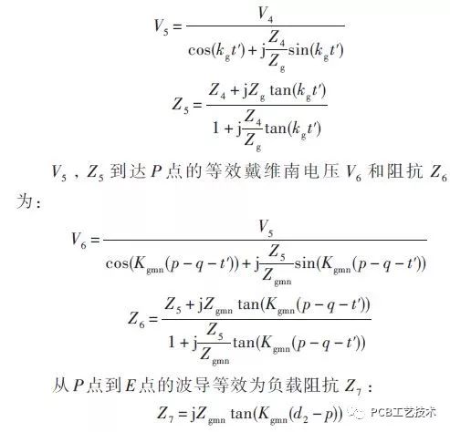
The voltage of each mode wave at point P is:
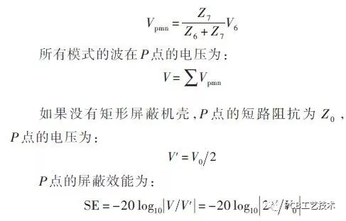
2 Simulation results analysis
In order to verify the correctness of the theoretical results, a rectangular shield shell with a thickness of 1 mm is irradiated by a plane electromagnetic wave with an electric field strength of 1 V - m-1. The cavity size is 300 mm × 120 mm × 600 mm, of which the front cavity length is 300. Mm , the rear cavity is 300 mm long, the hole size is 80 mm × 20 mm, the dielectric plate size is 300 mm × 120 mm × 1 mm, and it is installed at a distance of 100 mm from the second hole. The simulation frequency is 200 MHz~1. GHz .
The center of the dielectric plate is in a straight line with the opening center and the observation point. When there is a dielectric plate in the shielding cavity, the incident wave is coupled into the cavity, and the dielectric plate is encountered, and the dielectric loss occurs. The electromagnetic wave energy is mainly divided into three parts: a part of the transmission The dielectric plate is further propagated, a portion of the reflection, and a portion is diffracted through the gap between the dielectric plate and the cavity, and the dielectric plate also absorbs energy. Due to the transmission and diffraction of electromagnetic waves, an electromagnetic field is also present in the space behind the dielectric plate.
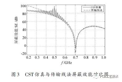
Figure 3 is a comparison of shielding effectiveness at the center point of the back cavity using the equivalent transmission line method and the CST simulation method. It can be seen that the results of the two methods are partially different at low frequencies, but are better after 300 MHz. And the cavity resonates at 707 MHz.
2.1 Change the influence of the size of the dielectric board on the shielding effectiveness
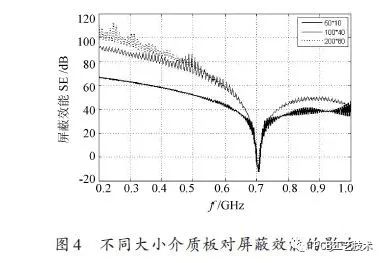
In Figure 4, the distance from the inner hole to the loading PCB is q=100 mm. Three different sizes of dielectric plates are used, which are 500 mm×10 mm, 100 mm×40 mm and 200 mm×80 mm. It can be seen that In a given frequency range, the larger the dielectric plate, the higher the shielding effectiveness of the cavity. This is because the larger the dielectric plate, the larger the dielectric loss, the smaller the field strength of the resonance point, and the greater the shielding effectiveness of the shielding body.
2.2 The effect of the distance between the dielectric plate and the second layer of holes on the shielding effectiveness
The dielectric plate size is not changed to 300 mm × 120 mm × 1 mm. The distance q of the inner hole to the loaded PCB is changed. Here q take 50 mm, 100 mm and 290 mm, respectively, and finally compare with the case without PCB.
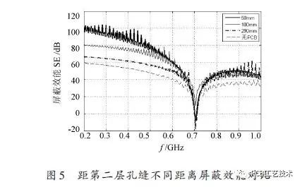
It can be seen from Fig. 5 that the farther the dielectric plate is from the second layer of the slit in a given frequency range, the lower the shielding effectiveness. When the dielectric plate is 50 mm away from the second layer of the hole, most of the coupling field is reflected and coupled out of the cavity, so the center strength of the second layer cavity is the smallest, and the shielding effectiveness is the largest, as the distance increases. Large, the field strength of the cavity is also gradually increased. When it is increased to 290 mm, the field strength of the cavity reaches the maximum value, which is close to the field strength when there is no dielectric plate, and the shielding effectiveness is also close to that of the non-dielectric plate.
2.3 Influence of the number of dielectric plates on shielding effectiveness
The dielectric plate size is 300 mm × 120 mm × 1 mm. When there is only one dielectric plate, it is placed 100 mm from the second hole, ie q=100 mm in Figure 1; when there are two When the dielectric plate is placed 50 mm and 100 mm from the second layer of the hole, ie q=50 mm and q=100 mm in Figure 1, when there are three dielectric plates, the distance is placed second. Where the hole is 50 mm, 100 mm and 150 mm, ie q=50 mm, q=100 mm and q=150 mm in Figure 1. The simulation results are shown in Figure 6.
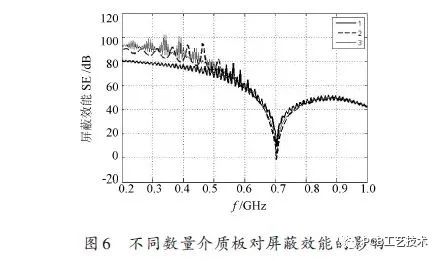
It can be seen from Fig. 6 that as the number of dielectric plates increases, the shielding effectiveness of the center position of the cavity increases.
2.4 Influence of different placement methods of dielectric plates on shielding effectiveness
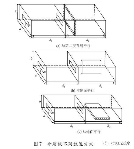
The size of the dielectric plate is the same, placed in three different ways: parallel to the second layer of the hole, placed 100 mm from the second layer of the hole; parallel to the side, placed in the center of the long side of the hole Position; parallel to the ground, placed in a position perpendicular to the center of the short side of the slot. The three placement methods are shown in Figure 7.
The simulation results of the three cases are shown in Figure 8.
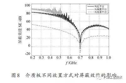
It can be seen from Fig. 8 that the shielding performance is the worst when the dielectric plates are placed in parallel with the ground, and the other two placement methods have little effect on the shielding effectiveness.
3 Impact of loading integrated operational amplifier board on shielding effectiveness
There is still a difference between the actual printed circuit board and the equivalent macroscopic dielectric board. Here, the macro dielectric board is replaced with an integrated operational amplifier board, as shown in FIG.
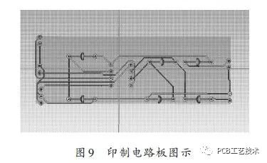
Comparing the influence of the dielectric plate and the circuit board on the shielding effectiveness in the shielding cavity, the dielectric plate size is the same as that of the circuit board, which are 75.59 mm×25.69 mm×0.711 2 mm, and the model is placed in the center of the shielding cavity. Origin - 99.288 8 mm position, where the dielectric plate is the macroscopic dielectric plate with the conductivity σ = 0.22 S - m-1 and the dielectric constant εr = 2.65. The printed circuit board is shown in Figure 9. Load the board of the integrated operational amplifier circuit. Using CST, the PCB model of the board is introduced into the microwave studio of CST. After simulation, the result is shown in Fig. 10.
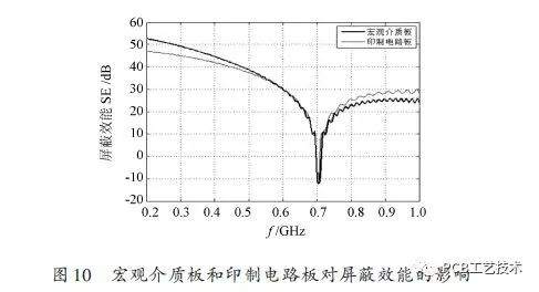
It can be seen from Fig. 10 that in the case of the same size, thickness, and placement position, the shielding performance obtained by the macroscopic dielectric board and the printed circuit board is not much different, that is, the error of replacing the printed circuit board with the macroscopic dielectric board is small.
After the printed circuit board is loaded, the shielding effectiveness of the cavity is mainly reflected in the variation of the electric field strength on the surface of the circuit board and the difference in surface current. The following results are obtained by CST simulation.
3.1 Circuit board surface electric field
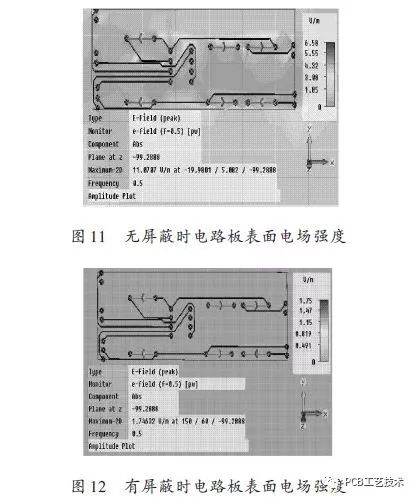
It can be seen from Fig. 11 and Fig. 12 that the maximum field strength is 11.070 7 V·m-1 when there is no shielding, and the maximum field strength is 0.164 V·m-1 when there is shielding. It can be seen that the shielding cavity has a good shielding effect on the circuit board. . And the wires that are close to each other are likely to cause high field strength. If there is no shielding, it will cause normal operation of the circuit board and cause damage in severe cases.
3.2 Board surface current
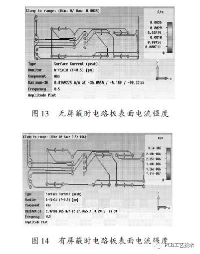
In Figure 13, the maximum surface current of the board is 0.014 93 A·m-1 when there is no shielding. In Figure 14, the maximum surface current of the board is 2.091 8e - 005 A·m-1 when there is shielding, which is obviously less than The shielding time is much reduced, indicating that the shielding cavity has a good shielding effect on the circuit board.
4 Conclusion
In this paper, the calculation formula of the shielding effectiveness of the rectangular cavity of the double-layer loading circuit board is introduced by the transmission line equivalent model. The correctness of the formula is verified by simulation, and the conclusion is drawn that the larger the dielectric plate is, the cavity shielding in a given frequency range. The higher the efficiency; the closer the dielectric plate is to the second layer, the higher the shielding effectiveness; the more the number of dielectric plates, the higher the shielding effectiveness; the shielding effectiveness is the worst when the dielectric plates are placed parallel to the ground, and the other two placement methods are shielded. There is little difference in performance impact. Through the above conclusions, when designing the casing, the shielding effectiveness of the system can be improved by rationally arranging the internal circuit board, and at the same time, the response frequency of the circuit in the cavity should avoid the resonant frequency of the cavity. In this paper, in order to be more suitable for practical applications, the equivalent dielectric board is replaced with the printed circuit board model loaded with the integrated operational amplifier circuit. The effectiveness of the macro dielectric board equivalent to the printed circuit board is verified by CST simulation. Similarity, and verify the shielding effect of the shield cavity on the internal circuit board and the effect of the shield cavity on the board function.
Pvc Trunking,Pvc Cable Trunking,Plastic Cable Trunking,Pvc Electrical Trunking
FOSHAN SHUNDE LANGLI HARDWARE ELECTRICAL CO.LTD , https://www.langliplastic.com
