
Recently, ARM has further disclosed some information about ML Procesor. EETimes' article "Arm Gives Glimpse of AI Core"[1] and AnandTech's article "ARM Details "Project Trillium" Machine Learning Processor Architecture" introduces them from different angles, which are worthy of our careful analysis.
ARM disclosed its ML Processor on the eve of the Spring Festival this year. At that time, there was not much information released. I also did a simple analysis (AI chip starts the year).
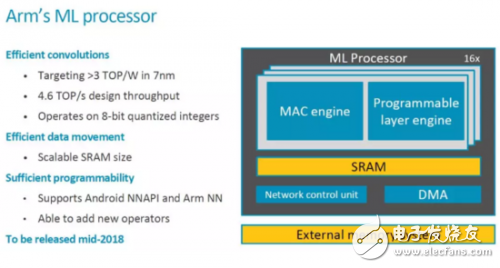
This time ARM has released more information, let's take a look. The first is the key Feature and some important information, which will be Released in mid-2018.
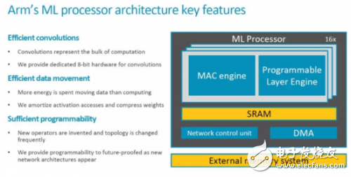
Top-level architecture
Compared with the basic block diagram originally announced, we have seen a more detailed block diagram and connection relationship of the modules this time, as shown in the figure below.
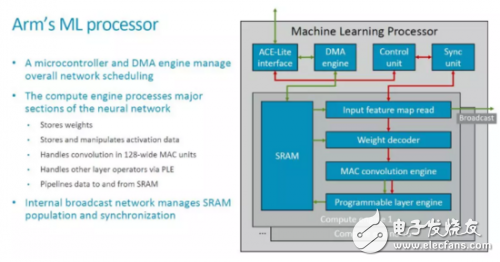
The top layer of MLP is a typical hardware accelerator to the outside. It has a local SRAM and interacts with external data and main control information (instructions) through an ACE-Lite interface. In addition, there should be some control signals, which are probably omitted here (refer to Nvidia's NVDLA).
In the above figure, the green arrow should indicate the data flow, and the red indicates the control flow. The CE in MLP shares a set of DMA, Control Unit and Sync Unit. Its basic processing flow is roughly as follows: 1. Configure Control Unit and DMA Engine; 2. DMA Engine reads data from external (such as DDR) and stores it locally In SRAM; 3. Input Feature Map Read module and Weight Read module read the feature map and weight to be calculated, process (such as decompression of Weight), and send to MAC ConvoluTIon Engine (hereinafter referred to as MCE); 4. MCE Perform operations such as convolution, and transfer the results to the Programmable Layer Engine (hereafter referred to as PLE); 5. PLE performs other processing and writes the results back to the local SRAM; 6. DMA Engine transfers the results to the external storage space (such as DDR ).
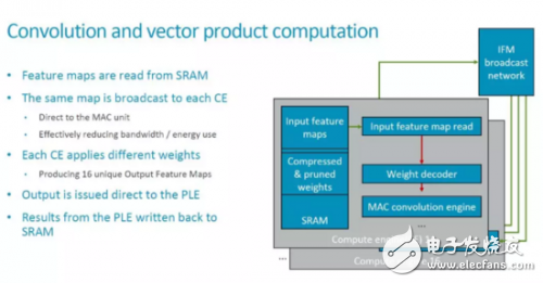
The Broadcast interface marked on the top layer realizes the function of broadcasting feature map data among multiple Compute Engines (hereinafter referred to as CE). Therefore, the basic convolution operation mode is that the same feature map is broadcast to multiple CEs, and different CEs use different weights to perform operations on these feature maps.
From the current configuration, MLP includes 16 compute engines, each with 128 MACs, that is, a total of 16x128=2048 MACs, and each cycle can perform 4096 operations. If you want to achieve the total processing capacity of 4.6TOPS as described by ARM, the clock cycle needs to reach about 1.12GHz. Since this indicator is for the 7nm process, it is not a big problem.
MCE achieves efficient convolutionIn the MLP architecture, MCE and PLE are the most important functional modules. MCE provides the main computing power (processing 90% of the computing), which should also be the largest area and power consumption part of the MLP. Therefore, one of the main goals of MCE design optimization is to achieve efficient convolution operations. Specifically, the design of MLP mainly considers the following methods, most of which we have discussed before.
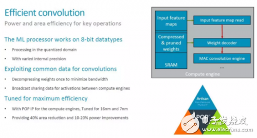
A more interesting point is the "varied internal precision" mentioned above. The specific meaning is not yet clear. However, the application should see a fixed 8bit data type. As for the support for low precision Inference, the information provided in [1] is, "The team is tracking research on data types down to 1-bit precision, including a novel 8-bit proposal from Microsoft. So far, the alternaTIves lack support in tools to make them commercially viable, said Laudick.†Therefore, in the first version of MLP, you should not see low precision or Bit-serial MAC (refer to the Bit-serial Processing that appeared on ISSCC2018 in the AI ​​chip in the year Introduction).
In addition, data compression and process optimization are also the main means to improve overall efficiency. Especially the optimization of the process, combined with ARM's process library, should have a better effect, which is where ARM has an advantage.
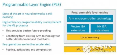
PLE achieves efficient programmabilityAs shown in the figure below, the structure of PLE basically expands the Vector processing and NN processing instructions on the basis of an ARM MCU. When discussing programmability, the main starting point is that the NN algorithm and architecture are still evolving.
We have analyzed the basic workflow of the entire MLP before, and MCE transmits the result to PLE after completing the calculation. It can be seen from this that the MCE should send the result to the Vector Register File (VRF), and then generate an interrupt to notify the CPU. After that, the CPU starts the Vector Engine to process the data. The details are shown in the figure below.
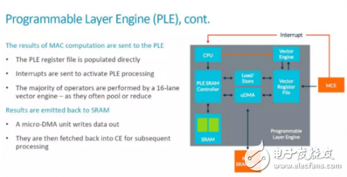
For students who are dedicated processors, this scalar CPU+vector engine architecture is not unfamiliar. Here, there is a Load/Store unit and uDMA between the local SRAM, VRF and Maing SRAM Unit (SRAM in CE) outside of PLE to realize data transmission, and the data flow is also relatively flexible. On the whole, in MLP, each CE has a PLE and MCE cooperation, that is, each MCE (128 MAC) corresponds to a programmable architecture. Therefore, the programmability and flexibility of ARM MLP is much higher than that of Google TPU1 and Nvidia's NVDLA. Of course, flexibility also means more additional overhead, as pointed out in [1], "The programmable layer engine (PLE) on each slice of the core offers "just enough programmability to perform [neural-net] manipulaTIons "" . High-efficient Programmability is one of the main selling points of MLP, and whether ARM's "just enough" is really the most suitable choice remains to be seen.
Lens Caps,Lens Cover,Camera Lens Cover,Camera Lens Cap
SHAOXING COLORBEE PLASTIC CO.,LTD , https://www.colorbeephoto.com