Power amplifier (Power Amplifier, referred to as PA) is called the "amplifier". It is the most basic equipment in the sound system. Its task is to carry out the weak electrical signal from the signal source (the professional sound system is from the mixer). Zoom in to drive the speaker to make a sound.
Characteristics of mobile phone amplifiers
The GSM/GPRS quad-band mobile phone transmits signals according to the communication standard of ETSI/3GPP, so the characteristics of the power amplifier must meet the following requirements.
In general, the output power level of PA is in the GSM850MHz/900MHz frequency band, which is divided into 15 power levels ranging from 5 (33dBm) to 19 (5dBm). In the DCS1800MHz/PCS1900MHz frequency band, there are 0 (30dBm)~15 (0dBm). Waiting for sixteen power levels, as the distance between the mobile phone and the neighboring base station and the receiving status of the mobile phone, the output power level of the PA must be relatively adjusted and accurately set according to the indication of the base station, not only a single output power.
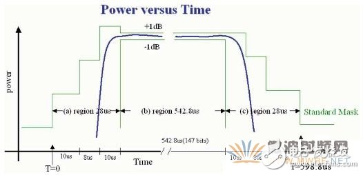
Because the GSM/GPRS communication system is a TDMA system (me-Division-mulple-Access), the signal transmission (up-Link) and reception (down-Link) do not occur at the same time, and the PA is mainly responsible for transmitting the mobile phone signal. To the base station, its PA power operation response time must comply with the specifications of the ETSI/3GPP communication standard, as shown in Figure 1, divided into three time zones (a) 28us (b) 542.8us (c) 28us, in the (a) area, When the mobile phone wants to transmit signals to the base station, the PA must be ready for Power-ramping-up within 28us to keep the PA output power at a stable and fixed value in order to start the real mobile signal transmission work. (b) Area, and when the signal is transmitted, the Power-ramping-down must be done in the (c) area 28us to turn off the PA Power to save battery current consumption while entering the receiving mode (receiving the base station signal). There are two points worth mentioning:
(1) In the areas (a) and (c), the reaction speed of the PA should be fast enough so that the PA can reach the full power output and the no power output of the PA within 28us, respectively, and the rate of increase of the power output (ramping- Up) or ramping-down must also have the appropriate speed to achieve a very smooth power rise and fall curve, otherwise it is easy to produce so-called switching spectrum noise, which in turn affects the call quality of neighboring mobile phone users.
(2) In the (b) region, the output power of the PA must be maintained very stable, and the power variation range is within ±1 dB. Otherwise, the signal to be transmitted by the mobile phone is easily changed by the PA itself due to the instability of the PA itself. The modulation spectrum noise is generated, which will greatly improve the BER (Bit-error-rate) of the mobile phone itself, and the call quality is not good.

Because the mobile phone and the base station have a maximum distance of about 35 kilometers, the output power of the PA is about 30~35dBm, so the PA needs a large supply current, and the current can be as high as 1.6~2A, and the output efficiency of the general PA is about 50%. In addition, when the PA duty cycle is applied to the GPRS Class 12 application, it will reach 50% (4 time slots), so the PA module will generate a lot of heat in the IC itself, so it must have good heat dissipation. Handle, otherwise the PA is easily damaged by overheating.
Because the mobile phone itself is often used in a rather unfavorable environment, such as high-speed driving, bad weather environment, etc., the receiving sensitivity of the mobile phone itself is very high, and at the same time, the output power required by the PA is compared. High, so the requirements for the characteristics of the receiving band noise power generated by the PA during operation will be more stringent.
Generally, in the normal operation mode of the mobile phone PA, the impedance seen at the output is 50Ω load, but when the mobile phone user improperly uses the mobile phone, such as holding the antenna or even unplugging the antenna, the PA load impedance will completely deviate from normal operation. 50Ω load, this is the so-called PA mismatch. Under such conditions, the PA power cannot be sent out, which will cause more heat to be scattered on the IC, which will easily lead to PA burnout. In addition, because the PA itself is large Power components, in addition to the output power, will generate a lot of thermal noise, PA itself will have a great stability problem, if the mismatch occurs again, it is more likely to cause PA oscillation, resulting in other frequency noise (SpuriousOscillaon noise) It affects other mobile phone system users, so the PA design itself must ensure that the PA does not oscillate and burn out under mismatch conditions.
As mentioned in the previous point, the PA is a high-power component, and its output power is impedance matching using a microstrip transmission line, so the RF signal is easily radiated to the PA peripheral mobile communication circuit via the medium coupling and air, and even affects Close to mobile phone users. The most typical example is that the signal is coupled to the VCO in the PLL, which is likely to cause the frequency offset of the VCO, which will greatly affect the call quality of the mobile phone itself. Therefore, the disadvantages and isolation of the PA design itself are a challenging subject.
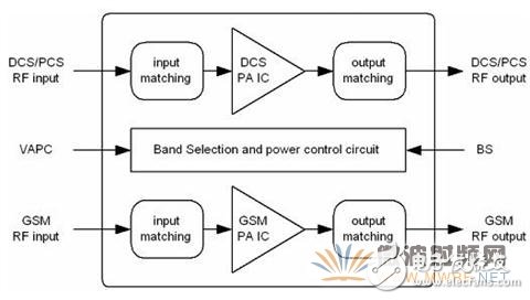
PA technology and operation PA design In recent years, due to the poor Q value of the IC output impedance matching line, the multi-chip module (MCU, Multi-Chip-Module) structure is used, as shown in Fig. 2.

Figure 2 Functional block diagram of PA
The function includes the following three parts:
50Ω input/output matching line: for proper impedance matching and power transfer with peripheral circuits such as voltage controlled oscillators and switchers.
CMOS power control IC: This IC can be said to be the core of the PA module. Its functions include: providing HBT IC DC bias (DC-Bias), band selection (Band-Selection between GSM and DCSBand), temperature compensation, self-power measurement (ensuring The output power of the PA is the base station demand value), the output power is adjusted (different output power level adjustment), the power switch (switching between transmission and reception) and the protection device circuit (avoiding the improper use of the mobile phone and causing damage) .
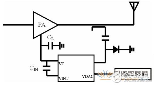
GSM/DCS HBT PA IC: The main function of this HBT PA IC is the power amplification of RF signals. Currently, mobile phone PA is manufactured by GaAs Hetero-Junction-Bipolar-Transistor HBT. . In application, the PA must be equipped with a control loop to make it fully compliant with the E-GSM/DCS/PCS standard, as shown in Figure 3.

Figure 3 power control loop
In use, a VDAC value is sent through the baseband to set the power value that the PA needs to transmit, and then the sensing Schottky diode is used to measure the output power of the PA, and the measured value is compared with the value of the VDAC to obtain an error. The current is then integrated by the integrator Cin to determine the output voltage of the VC. Then, the voltage value of the VC is used to adjust the amplification power of the PA, thus forming a stable control loop system to ensure that the PA output power is set by the baseband. Power value.
Lszh Wire,Lszh Grounding Wire,Lsoh Grounding Wire,Lshf Grounding Wire
Baosheng Science&Technology Innovation Co.,Ltd , https://www.bscables.com
