
The MAX6954 is a universal display driver that can control multiple discrete, 7-segment, 14-segment, or 16-segment LED displays via a serial port. This application note describes typical applications and configurations for driving 8-bit monochrome, 16-segment LED displays.
For more information about MAX6954, please refer to the MAX6954 data sheet.
The application notes "Quick Start: Using the MAX6954 to Drive a 7-Segment LED Display" and "Quick Start: Using the MAX6954 to Drive a 14-Segment LED Display" Similar to this article, they explain how to configure the MAX6954 to drive a 7-segment and 14-segment display, respectively.
A common application of the MAX6954 is to drive up to 8-bit 16-segment monochrome LEDs. This application note guides the user how to connect the MAX6954 to a 16-segment display, and how to configure its internal registers to control the display of 104 characters in a built-in font.
The MAX6954 uses a multiplexing technique that alternates the polarity of the driver port to reduce the number of pins. This is different from the standard LED multiplexing connection used separately for the cathode and anode pins of the driver. The application note "Charlieplexing-Reduced Pin-Count LED Display MulTIplexing" discusses this technology. Table 1 shows the connection table between MAX6954 and 16-segment display. This table is compatible with the MAX6954 multiplexing configuration and its 104-character built-in font. The letters in Table 1 correspond to the segment identifiers in Figure 2. Figure 1 is a schematic diagram of the MAX6954 driving an eight-bit 16-segment display. 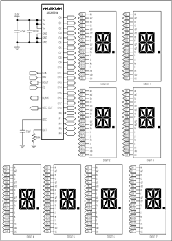
Enlarged display Figure 1. MAX6954 16-segment display application circuit 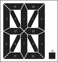
Figure 2. Segment identification of the 16-segment display
Table 1. Connection table with eight 16-segment displays
| DIGIT | O0 | O1 | O2 | O3 | O4 | O5 | O6 | O7 | O8 | O9 | O10 | O11 | O12 | O13 | O14 | O15 | O16 | O17 | O18 |
| 0 | CCO | - | a1 | a2 | b | c | d1 | d2 | e | f | g1 | g2 | h | i | j | k | l | m | dp |
| 1 | - | CC1 | a1 | a2 | b | c | d1 | d2 | e | f | g1 | g2 | h | i | j | k | l | m | dp |
| 2 | a1 | a2 | CC2 | - | b | c | d1 | d2 | e | f | g1 | g2 | h | i | j | k | l | m | dp |
| 3 | a1 | a2 | - | CC3 | b | c | d1 | d2 | e | f | g1 | g2 | h | i | j | k | l | m | dp |
| 4 | a1 | a2 | b | c | CC4 | - | d1 | d2 | e | f | g1 | g2 | h | i | j | k | l | m | dp |
| 5 | a1 | a2 | b | c | - | CC5 | d1 | d2 | e | f | g1 | g2 | h | i | j | k | l | m | dp |
| 6 | a1 | a2 | b | c | d1 | d2 | CC6 | - | e | f | g1 | g2 | h | i | j | k | l | m | dp |
| 7 | a1 | a2 | b | c | d1 | d2 | - | CC7 | e | f | g1 | g2 | h | i | j | k | l | m | dp |
After the MAX6954 is connected to the 16-segment display, the display test mode can be used to check the correctness of the connection. The display test mode is not affected by the control and data registers, and lights all segments of the display, but does not change any register contents. Write 0x01 to register 0x07 to start the display test mode. In the test mode, if there is an unlit segment on the display, the connection is incorrect. Write 0x00 to register 0x07 to exit display test mode.
After completing the connection check, you need to set the MAX6954 register value as required to drive the 16-segment display. Table 2 includes the power-on initial values ​​of some important registers of MAX6954. The MAX6954 is in power-down mode when it is first powered on. Everyone displays blanking, selects a 16-segment font and sets the maximum number of scan digits, that is, eight bits. The default values ​​of the decoding mode register (0x01) and number type (0x0C) are applicable to the 16-segment display.
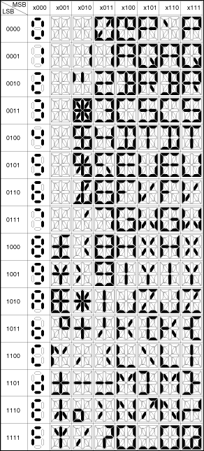
Figure 3. 16-segment display font
Table 2. MAX6954 initial state of registers after power-up
| REGISTER | POWER-UP CONDITION | ADDRESS (HEX) | REGISTER DATA | |||||||
| D7 | D6 | D5 | D4 | D3 | D2 | D1 | D0 | |||
| Decode Mode | 16-segment font enabled | 0x01 | 1 | 1 | 1 | 1 | 1 | 1 | 1 | 1 |
| Global Intensity | 1/16 (minimum intensity) | 0x02 | X | X | X | X | 0 | 0 | 0 | 0 |
| Scan Limit | Display eight 16-segment digits: 0, 1, 2, 3, 4, 5, 6, 7 | 0x03 | X | X | X | X | X | 1 | 1 | 1 |
| Control Register | Shutdown enabled, blink disabled, blink speed is slow | 0x04 | 0 | 0 | X | X | 0 | 0 | 0 | 0 |
| Display Test | Normal operaTIon (display test disabled) | 0x07 | X | X | X | X | X | X | X | 0 |
| Digit Type | Digits 0 through 7 are 16 segment digits | 0x0C | 0 | 0 | 0 | 0 | 0 | 0 | 0 | 0 |
| Intensity10 | 1/16 (min on), digits 1 and 0 | 0x10 | 0 | 0 | 0 | 0 | 0 | 0 | 0 | 0 |
| Intensity32 | 1/16 (min on), digits 3 and 2 | 0x11 | 0 | 0 | 0 | 0 | 0 | 0 | 0 | 0 |
| Intensity54 | 1/16 (min on), digits 5 and 4 | 0x12 | 0 | 0 | 0 | 0 | 0 | 0 | 0 | 0 |
| Intensity76 | 1/16 (min on), digits 7 and 6 | 0x13 | 0 | 0 | 0 | 0 | 0 | 0 | 0 | 0 |
| Digit 0 | Blank digit, both planes | 0x60 | 0 | 0 | 1 | 0 | 0 | 0 | 0 | 0 |
| Digit 1 | Blank digit, both planes | 0x61 | 0 | 0 | 1 | 0 | 0 | 0 | 0 | 0 |
| Digit 2 | Blank digit, both planes | 0x62 | 0 | 0 | 1 | 0 | 0 | 0 | 0 | 0 |
| Digit 3 | Blank digit, both planes | 0x63 | 0 | 0 | 1 | 0 | 0 | 0 | 0 | 0 |
| Digit 4 | Blank digit, both planes | 0x64 | 0 | 0 | 1 | 0 | 0 | 0 | 0 | 0 |
| Digit 5 | Blank digit, both planes | 0x65 | 0 | 0 | 1 | 0 | 0 | 0 | 0 | 0 |
| Digit 6 | Blank digit, both planes | 0x66 | 0 | 0 | 1 | 0 | 0 | 0 | 0 | 0 |
| Digit 7 | Blank digit, both planes | 0x67 | 0 | 0 | 1 | 0 | 0 | 0 | 0 | 0 |
The configuration register (0x04) is used to set the entry and exit of the shutdown mode, control the blinking function, globally clear the data of each bit, and select whether to control the brightness of each bit globally or individually. The configuration register contains 7 bits (see Table 3). The S bit is used to select power-down mode or normal operating mode (read / write). Bit B is used to select the blinking rate (read / write). The E bit is used to globally enable or disable the flashing function (read / write). The T bit is used to reset the blinking sequence (this data is not stored-transient bit). The R bit is used to globally clear the P0 and P1 two-level registers corresponding to all display bits (this data is not stored-transient bit). The I bit is used to select whether the brightness of each bit is controlled globally or individually (read / write). The P bit is used to return to the current blink timing phase (read-only-writing to this bit will be ignored). Table 3. Configuration register format
| CONFIGURATION REGISTER DATA BIT | DATA BIT LABEL | STATE | FUNCTION |
| D7 | P | 0 | P1 Blink Phase |
| 1 | P0 Blink Phase | ||
| D6 | I | 0 | Intensity for all digits is controlled by one setting in the Global Intensity Register |
| 1 | Intensity for digits is controlled by the individual settings in the Intensity10 through Intensity76 registers. | ||
| D5 | R | 0 | Digit data for both planes P0 and P1 are unaffected |
| 1 | Digit data for both planes P0 and P1 are cleared on the rising edge of active-low CS | ||
| D4 | T | 0 | Blink timing counters are unaffected. |
| 1 | Blink timing counters are reset on the rising edge of active-low CS. | ||
| D3 | E | 0 | Blink function disabled |
| 1 | Blink function enabled | ||
| D2 | B | 0 | Slow Blinking. Segments blink on for 1s, off for 1s with fOSC = 4MHz. |
| 1 | Fast Blinking. Segments blink on for 0.5s, off for 0.5s with fOSC = 4MHz. | ||
| D1 | X | X | Don't care |
| D0 | S | 0 | Shutdown |
| 1 | Normal Operation |
Start the display driver by writing 0x01 to register 0x04, and at the same time set the working mode to global brightness control and prohibit flashing. The internal oscillator starts when the MAX6954 exits shutdown mode, and the oscillator output pin is OSC_OUT. Note that when the power-on state of the data control registers 0x60 to 0x67 is 0x20 or no segment is lit, the 16-segment display remains blanked (see Table 2 and Figure 3).
The MAX6954 has a built-in 104-character ASCII font for 16-segment displays. The characters are the sum of standard ASCII characters
 These common symbols. The 104 characters are represented by 7 digits, and the 8th digit is used to select whether to light the decimal point (DP) (see Table 4). The data register has two levels, P0 and P1. Each display bit is represented by 2 bytes in the memory, one byte is located at P0 and the other is located at P1 (see Table 7). The data register is a mapped address mode, so each bit of data can be updated in P0 (registers 0x20 to 0x27), P1 (registers 0x40 to 0x47), and it can also be updated in two levels (registers 0x60 to 0x67). The data in the data register does not directly control the display of each segment in the 16-segment display. Instead, it is used to address a character generator that stores 16-segment font data (see Figure 3). The lower 7 bits of the register data (D6 to D0) are used to select characters from the font. The highest digit (D7) controls the decimal point (DP) display; set to 1 to display DP, and set to 0 to not display DP.
 Table 4. Digital type data register format
| MODE | ADDRESS CODE (HEX) | REGISTER DATA | ||||||||
| D7 | D6 | D5 | D4 | D3 | D2 | D1 | D0 | |||
| 16-segment mode, writing digit data to use font map data with decimal place unlit | 0x20 to 0x27 0x40 to 0x47 0x60 to 0x67 | 0 | Bits D6 to D0 select font character 0 to 127 | |||||||
| 16-segment mode, writing digit data to use font map data with decimal place lit | 0x20 to 0x27 0x40 to 0x47 0x60 to 0x67 | 1 | Bits D6 to D0 select font character 0 to 127 | |||||||
If the flash function is disabled by the configuration register flash enable bit E (see Table 3), the data in the data register in P0 is used for display multiplexing. The data in the data register in P1 is not used. If the blinking function is enabled, the data multiplexing display in P0 and P1 is used alternately. The data in P0 and P1 are applied to different phases of the blinking clock alternately changing, thereby multiplexing the LED display to achieve the blinking function.
The following is an example of using the MAX6954 driver to display eight characters, "MAXIM-IC". Set the configuration register to disable the flashing function, so that you can control data bits 0 to 7 by writing data to registers 0x20 to 0x27. Use the font diagram in Figure 3 to get the code corresponding to each character.
Table 5. MAXIM-IC display example
| REGISTER ADDRESS (HEX) | DIGIT | CHARACTER | FONT MAP EQUIVALENT CODE | |
| DECIMAL | HEX | |||
| 0x20 | 0 | M | 0100 1101 | 0x4D |
| 0x21 | 1 | A | 0100 0001 | 0x41 |
| 0x22 | 2 | X | 0101 1000 | 0x58 |
| 0x23 | 3 | I | 0100 1001 | 0x49 |
| 0x24 | 4 | M | 0100 1101 | 0x4D |
| 0x25 | 5 | - | 0010 1101 | 0x2D |
| 0x26 | 6 | I | 0100 1001 | 0x49 |
| 0x27 | 7 | C | 0100 0011 | 0x43 |
Adjust the display brightness by writing data to register 0x02 (global brightness control register). The brightness can be adjusted between 0x00 (minimum brightness, 1/16 current) and 0xFF (maximum brightness, 15/16 current). You can also individually control the brightness of each bit. For more information on display brightness adjustment and other advanced features (such as GPIO and key scan), please refer to the MAX6954 data sheet.
Table 6. Quick start routine instruction set
| REGISTER (HEX) | COMMAND (HEX) | FUNCTION |
| 0x07 | 0x01 | Enter display test mode |
| 0x07 | 0x00 | Exit display test mode |
| 0x04 | 0x01 | Exit shutdown mode, disable blinking and select global intensity control |
| 0x20 | 0x4D | Write "M" to digit 0 |
| 0x21 | 0x41 | Write "A" to digit 1 |
| 0x22 | 0x58 | Write "X" to digit 2 |
| 0x23 | 0x49 | Write "I" to digit 3 |
| 0x24 | 0x4D | Write "M" to digit 4 |
| 0x25 | 0x2D | Write "-" to digit 5 |
| 0x26 | 0x49 | Write "I." to digit 6 |
| 0x27 | 0x43 | Write "C" to digit 7 |
| 0x02 | 0xFF | Set globalk intensity to full-scale |
Table 7. MAX6954 / MAX6955 partial register address map
| REGISTER | ADDRESS (COMMAND BYTE) | ADDRESS (HEX CODE) | |||||||
| D15 | D14 | D13 | D12 | D11 | D10 | D9 | D8 | ||
| Decode Mode | R / active-low W | 0 | 0 | 0 | 0 | 0 | 0 | 1 | 0x01 |
| Global Intensity | R / active-low W | 0 | 0 | 0 | 0 | 0 | 1 | 0 | 0x02 |
| Scan Limit | R / active-low W | 0 | 0 | 0 | 0 | 0 | 1 | 1 | 0x03 |
| Configuration | R / active-low W | 0 | 0 | 0 | 0 | 1 | 0 | 0 | 0x04 |
| Display Test | R / active-low W | 0 | 0 | 0 | 0 | 1 | 1 | 1 | 0x07 |
| Digit Type | R / active-low W | 0 | 0 | 0 | 1 | 1 | 0 | 0 | 0x0C |
| Intensity 10 | R / active-low W | 0 | 0 | 1 | 0 | 0 | 0 | 0 | 0x10 |
| Intensity 32 | R / active-low W | 0 | 0 | 1 | 0 | 0 | 0 | 1 | 0x11 |
| Intensity 54 | R / active-low W | 0 | 0 | 1 | 0 | 0 | 1 | 0 | 0x12 |
| Intensity 76 | R / active-low W | 0 | 0 | 1 | 0 | 0 | 1 | 1 | 0x13 |
| Digit 0 Plane P0 | R / active-low W | 0 | 1 | 0 | 0 | 0 | 0 | 0 | 0x20 |
| Digit 1 Plane P0 | R / active-low W | 0 | 1 | 0 | 0 | 0 | 0 | 1 | 0x21 |
| Digit 2 Plane P0 | R / active-low W | 0 | 1 | 0 | 0 | 0 | 1 | 0 | 0x22 |
| Digit 3 Plane P0 | R / active-low W | 0 | 1 | 0 | 0 | 0 | 1 | 1 | 0x23 |
| Digit 4 Plane P0 | R / active-low W | 0 | 1 | 0 | 0 | 1 | 0 | 0 | 0x24 |
| Digit 5 ​​Plane P0 | R / active-low W | 0 | 1 | 0 | 0 | 1 | 0 | 1 | 0x25 |
| Digit 6 Plane P0 | R / active-low W | 0 | 1 | 0 | 0 | 1 | 1 | 0 | 0x26 |
| Digit 7 Plane P0 | R / active-low W | 0 | 1 | 0 | 0 | 1 | 1 | 1 | 0x27 |
| Digit 0 Plane P1 | R / active-low W | 1 | 0 | 0 | 0 | 0 | 0 | 0 | 0x40 |
| Digit 1 Plane P1 | R / active-low W | 1 | 0 | 0 | 0 | 0 | 0 | 1 | 0x41 |
| Digit 2 Plane P1 | R / active-low W | 1 | 0 | 0 | 0 | 0 | 1 | 0 | 0x42 |
| Digit 3 Plane P1 | R / active-low W | 1 | 0 | 0 | 0 | 0 | 1 | 1 | 0x43 |
| Digit 4 Plane P1 | R / active-low W | 1 | 0 | 0 | 0 | 1 | 0 | 0 | 0x44 |
| Digit 5 ​​Plane P1 | R / active-low W | 1 | 0 | 0 | 0 | 1 | 0 | 1 | 0x45 |
| Digit 6 Plane P1 | R / active-low W | 1 | 0 | 0 | 0 | 1 | 1 | 0 | 0x46 |
| Digit 7 Plane P1 | R / active-low W | 1 | 0 | 0 | 0 | 1 | 1 | 1 | 0x47 |
Blue Bluetooth Headset is very simple and easy to operate with one hand to realize multi-functions by just touching the earbuds,Conveniently with our Built-in Microphone on earbuds with CSR chip. Noise Cancellation for safe and sound One-Touch Hands-free Calling so you don't have to stop biking, running, walking, or driving. Ould be connected as a pair or used each separately. Glad to share one for your friend or your family. Music sharing with true free.
We are the Top Chinese manufacturer of Black Bluetooth Headset , and looking forward to cooperate with you!
Blue Bluetooth Headset
Blue Bluetooth Headset,Stereo Wireless Earbuds,Sport Running Earphones,Earphones With Microphone
ShenDaDian(China) Digital Electronics Co.,Ltd , http://www.btearbuds.com