
In the high frequency field, signals or electromagnetic waves must propagate along a transmission path with a uniform characteristic impedance. When an impedance mismatch or discontinuity is encountered, a portion of the signal will be reflected back to the transmitter and the remaining portion of the electromagnetic wave will continue to be transmitted to the receiver. The degree of signal reflection and attenuation depends on the degree of impedance discontinuity. As the magnitude of the mismatch impedance increases, a larger portion of the signal is reflected and more attenuation or degradation is observed at the receiving end.
Impedance mismatch is often encountered in SMT pads, board-to-board connectors, and cable-to-board connectors (such as SMA) with AC-coupled (also known as DC-blocking) capacitors.
In the case of the AC-coupling capacitor SMT pad shown in Figure 1, the signal propagated along the PCB trace with a 100Ω differential impedance and a 5mil copper foil width, reaching a 30mil wide with a wider copper foil (such as a 0603 package) The SMT pad will encounter impedance discontinuities. This phenomenon can be explained by equations (1) and (2). An increase in the cross-sectional area or width of the copper foil will increase the strip capacitance, which in turn introduces a capacitive discontinuity, ie a negative surge, to the characteristic impedance of the transmission channel.
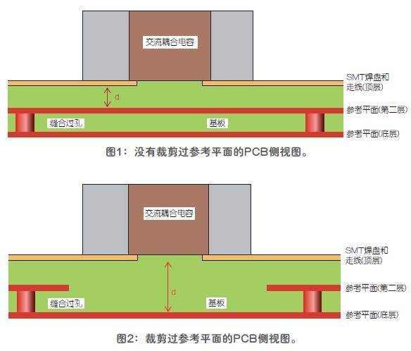
In order to minimize the discontinuity of the capacitor, it is necessary to trim the reference plane area directly below the SMT pad and create a copper fill on the inner layer, as shown in Figures 2 and 3, respectively. This increases the distance between the SMT pad and its reference plane or return path, thereby reducing capacitive discontinuities. Micro-stitched vias should also be inserted to provide electrical and physical connections between the original reference plane and the inner new reference copper foil to establish the correct signal return path to avoid EMI radiation problems.


However, the distance "d" should not increase too much, otherwise the strip inductor will exceed the strip capacitance and cause inductance discontinuities. Where: C = strip capacitor (unit: pF); L = strip inductor (unit: nH); Zo = characteristic impedance (unit: Ω); ε = dielectric constant; w = SMT pad width; l = SMT pad length; d = distance between the SMT pad and the lower reference plane; t = thickness of the SMT pad. The same concept can also be applied to SMT pads for board-to-board (B2B) and cable-to-board (C2B) connectors. The verification of the above concept will be completed by TDR and insertion loss analysis. The analysis was done by establishing a 3D model of the SMT pad in the EMPro software and then importing it into Keysight ADS for TDR and insertion loss simulation. Analysis of the SMT Pad Effect of AC Coupling Capacitors A 3D model of SMT with medium loss substrate is built in EMPro, where a pair of microstrip differential traces are 2 inches long and 5 mils wide, in single-ended mode with a distance of 3.5 mil from its reference plane. This pair of traces enters from one end of the 30 mil wide SMT pad and exits from the other end.

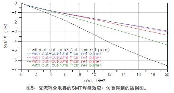
Figure 4 and Figure 5 show the simulated TDR and insertion loss graphs, respectively. The impedance mismatch caused by the unplanned SMT design of the reference plane is 12Ω, and the insertion loss is -6.5dB at 20GHz. Once the reference plane area under the SMT pad is cropped (where "d" is set to 10 mil), the mismatch impedance can be reduced to 2 Ω and the insertion loss at 20 GHz is reduced to -3 dB. Further increase of "d" will cause the strip inductor to exceed the capacitance, causing the inductor discontinuity, which in turn will cause the insertion loss to deteriorate (ie -4.5 dB). Analyze the SMT pad effect of a B2B connector. Create a 3D model of the SMT pad of a B2B connector in EMPro with a connector pitch of 20 mils, a lead width of 6 mils, and a pad connected to a pair of 5 inches long. It is 5 mils wide and uses a single-ended mode microstrip differential trace with a trace distance of 3.5 mils from its reference plane. The thickness of the SMT pad is 40 mils, and this thickness, including the connector pins and solder, is almost 40 times the thickness of the microstrip PCB trace.


An increase in copper thickness will result in a discontinuity in capacitance and a higher signal attenuation. This phenomenon can be seen in the TDR and insertion loss simulation diagrams shown in Figures 6 and 7, respectively. Impedance mismatch can be minimized by cutting out the copper area at the appropriate spacing "d" (ie 7 mils) directly below the SMT pad. Summary The analysis in this paper demonstrates that cropping the reference plane area directly below the SMT pad can reduce the impedance mismatch and increase the bandwidth of the transmission line. The distance between the SMT pad and the internal reference copper foil depends on the width of the SMT pad and the effective thickness of the SMT pad including the connector pins and solder. 3D modeling and simulation should be performed before the PCB is put into production to ensure good signal integrity of the constructed transmission channel.
Pharmaceuticals,2-Methyl- Propanoic Acid Monohydrate Price,2-Methyl- Propanoic Acid Monohydrate Free Sample,Pure 2-Methyl- Propanoic Acid Monohydrate
Zhejiang Wild Wind Pharmaceutical Co., Ltd. , https://www.wild-windchem.com