Summary:
UV LED light sources offer significant advantages over traditional UV light sources, including environmental friendliness, low power consumption, and selective wavelength emission. However, their application in the printing industry faces numerous challenges, particularly with reliability issues. Organic materials used in packaging often exhibit poor UV resistance and high moisture and oxygen permeability, which can lead to performance degradation and reduced device reliability. In contrast, all-inorganic UV LEDs based on CMH packaging technology are encapsulated in inorganic materials, providing excellent air tightness, high reliability, long lifespan, and low thermal resistance. Differences between COB (Chip On Board) and DOB (Device On Board) modules in terms of packaging materials and production processes result in distinct performance and reliability characteristics. The thermal resistance of the substrate insulation layer significantly affects COB modules, while the solder interconnection layer has a major impact on DOB modules. To address the issue of excessive voiding in the solder layer during mounting (typically above 20%), extensive experiments have led to optimal process parameters that reduce the void ratio to less than 100%, with more than 80% of voids around 5%. This greatly minimizes the impact of voids on the photothermal performance and reliability of UV LED devices.
Keywords: UV LED, printing industry, reliability, void rate
I. Introduction
In the 1860s, the first UV-curable ink was introduced. With the rapid development of UV curing technology, UV printing inks have found widespread use in various printing methods, such as digital printing, screen printing, lithography, flexography, and gravure printing. Traditionally, UV curing systems were paired with mercury lamps. However, due to increasing environmental concerns, traditional UV light sources are being phased out, leading to a surge in the market for Ultra-Violet Light Emitting Diodes (UV LEDs).
Compared to conventional UV light sources, UV LEDs offer several benefits, including energy efficiency, longer lifespan, lower power consumption, and precise wavelength selection. UV LEDs can be categorized into UVA (315–400 nm), UVB (280–315 nm), and UVC (200–280 nm) based on their emission wavelengths. Generally, wavelengths above 300 nm are considered shallow UV, while those below 300 nm are classified as deep UV. UV LEDs can also be divided into discrete devices and integrated modules, such as COB (Chip On Board) and DOB (Device On Board). COB involves directly soldering multiple LED chips onto a substrate, while DOB encapsulates the chips first and then mounts them on the substrate.
As an emerging light source, UV LEDs face various challenges when applied in the printing industry. For example, organic materials exposed to UV energy may degrade, leading to issues like excessive ink surface exposure or insufficient curing. Additionally, harmful substances can infiltrate the light source, affecting its performance, and there are challenges related to wavelength matching, light uniformity, extraction efficiency, and overall reliability. Given the varying levels of packaging technology among LED manufacturers, the market is flooded with UV LED products of inconsistent quality, resulting in frequent reliability issues at the application end. This paper explores the reliability of UV LEDs in the printing industry from two perspectives: UV LED discrete devices and UV LED integrated modules.

Table 1 Several typical package products of UV LED
Second, UVLED Discrete Devices
As shown in Table 1, UV LED discrete devices can be categorized into those packaged with organic materials and those with inorganic materials. Organic material-packaged UV LEDs typically use materials like epoxy resin or silicone gel, while inorganic ones employ ceramics, glass, or metallic glass. These differences in materials lead to variations in performance, lifespan, and reliability. This section compares organic silica gel and inorganic glass in terms of transmission rate, thermal properties, reliability, air tightness, and electrical properties.
(1) Transmission Rate
The transmittance of the encapsulating material directly impacts the light output of UV LEDs. Glass generally exhibits higher transmittance across the UV spectrum compared to organic silica gels. After UV exposure, the transmittance of organic materials drops significantly, whereas glass remains stable. This makes glass a better choice for UV applications.
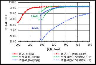
Figure 1. Transmission of typical organic and inorganic materials before and after UV irradiation.
(2) Thermal Properties
Organic materials tend to degrade under heat and UV exposure, leading to yellowing, cracking, or peeling. In contrast, inorganic materials like glass show greater thermal stability. Experiments showed that phenyl silica gel turned yellow after baking, while glass remained unaffected.
(3) Reliability Test
Long-term UV exposure causes organic materials to degrade, reducing light output and reliability. Glass-encapsulated UV LEDs maintained higher light output and stability over time. Organic materials experienced faster degradation, especially in the deep UV range.
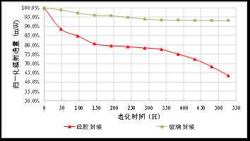
Figure 2 Radiation flux curve of UV LED normal temperature aging for typical organic and inorganic materials
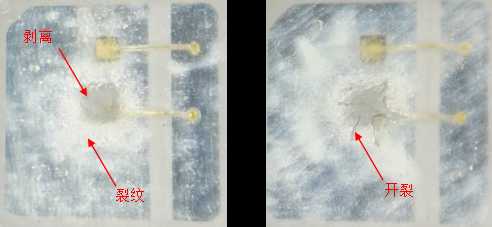
Figure 3. Appearance of a typical organic material package UV LED after normal temperature aging (336H on the left and 528H on the right)
(4) Air Tightness
Organic materials allow more moisture and oxygen to penetrate, reducing device reliability. Glass, being dense, provides superior air tightness.
(5) Electrical Properties
Organic materials may release ions or small molecules, potentially affecting the chip's electrical performance. Glass does not exhibit this issue.
In summary, inorganic materials outperform organic ones in most aspects. All-inorganic UV LEDs using CMH packaging technology offer excellent reliability and performance, making them suitable for harsh environments. These products are designed with ceramic substrates, metal and hard glass covers, and nitrogen-filled cavities to ensure hermetic sealing. They meet military standards for air tightness and avoid reliability issues caused by organic material degradation. Compared to other UV LED devices, they offer low thermal resistance, long life, and high reliability, making them ideal for various applications in the printing industry.
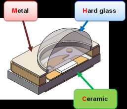
Figure 4 Schematic diagram of the full inorganic UV LED structure based on CMH packaging technology

Table 2 Product Performance Table
Third, UV LED Integrated Module
UV LED integrated modules on the market include COB and DOB. Their differences lie in packaging materials, production processes, optical performance, electrical performance, and thermal performance.
(1) Packaging Materials
COB and DOB differ in the choice of chips and substrates. COBs often use horizontal or vertical chips, while DOB primarily uses vertical chips. Copper and aluminum nitride (AlN) ceramic substrates are common. AlN substrates are more expensive and brittle, while copper substrates are more flexible and cost-effective.
(2) Production Process
COB is typically customized and harder to mass-produce, while DOB is standardized and easier to scale. Manufacturing defects in COB can lead to complete failure, whereas DOB only loses one device.
(4) Light Performance
Vertical structure chips allow higher current and optical power density, making them suitable for higher power applications. COBs using lateral chips are limited to low-power scenarios.
(5) Electrical Properties
DOB allows individual chip anti-static protection and testing, improving reliability and fault analysis.
(6) Thermal Properties
Heat dissipation paths vary between COB and DOB. COB has higher thermal resistance due to the insulating layer, while DOB’s thermal resistance depends on the solder layer. Poor solder joint quality increases thermal resistance, affecting performance and reliability. Studies show that even small voids in the solder layer can significantly increase thermal resistance.

(a) COB using a lateral structure UV LED chip

(b) COB using vertical structure UV LED chips
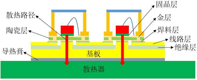
(c) DOB using vertical structure UV LED chips
Figure 5 Typical COB and DOB module structure
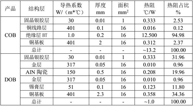
Table 3 Thermal resistance calculation of COB and DOB
The solder layer between the device and the substrate often contains voids, typically above 20%. Through extensive experiments, optimal process parameters were identified to control the void ratio within 100%, with over 80% of voids below 5%. This reduces the impact of voids on photothermal performance and reliability.
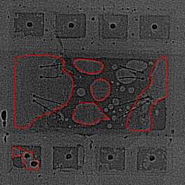
Figure 6 X-RAY scan of a typical DOB module
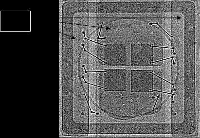
Figure 7 X-RAY scan of a typical DOB module after process optimization
Fourth, Summary
By analyzing UV LED discrete devices and integrated modules, it is clear that inorganic packaging materials outperform organic ones in terms of transmittance, air tightness, electrical properties, and thermal performance. Therefore, organic-packaged UV LEDs are suitable for low-demand applications, while all-inorganic UV LEDs based on CMH packaging technology are ideal for the printing industry. Additionally, through extensive research, optimal process parameters have been established to reduce the void rate in DOB modules to below 100%, with over 80% of voids at around 5%. This significantly improves the photothermal performance and reliability of UV LED devices.

Ethernet Network Connectors,Ethernet Cable Adapter,Ethernet Cable Connector,Internet Cable Connector
Dongguan Zhuoyuexin Automotive Electronics Co.,Ltd , https://www.zyx-fakra.com
