
Many young engineers initially turn to programmable logic when exploring design options in their projects. However, as the industry increasingly depends on programmable logic, certain challenges have emerged that are often not addressed in traditional circuit design education. This lack of awareness can lead to engineers creating systems without realizing there are alternative technologies that might be more efficient or cost-effective. The issue is closely tied to limited hands-on experience with different design approaches, which ultimately affects their ability to develop high-performance, low-cost solutions.
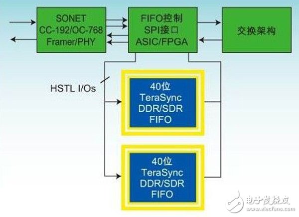
Figure 1: 40Gbps solution for high performance routers
A prime example of this trend is the use of embedded buffer memory. For years, FIFOs and multiport memories were the go-to choices for experienced engineers looking to build cost-effective data buffering systems. But with the growing memory capacity of FPGAs, many engineers now opt to use on-chip memory instead of discrete components. This shift is driven by the desire to reduce component count and save board space, making the system more compact and efficient.
For advanced applications, integrating functions like FIFOs or multiport memories directly into an FPGA makes sense. By combining multiple data buffers and control functions into a single chip, engineers can achieve better performance and reliability. To support this, FPGA manufacturers provide standardized IP blocks that help accelerate development and simplify the design process.
However, these benefits come at a price. High-density FPGAs are expensive, especially when dealing with data bus speeds above 100MHz or requiring higher buffer capacities. Performance can also become an issue. Some limitations, such as timing constraints or reduced throughput, may not be immediately apparent when integrating FIFO or multiport memory functions into programmable logic. In some cases, using discrete components or smaller FPGAs might offer a more optimal solution.
The problem often goes unnoticed. Because many educational programs emphasize programmable logic, today’s engineers may not be fully aware of the latest advancements in dedicated memory solutions like FIFOs and multiport memories. Modern FIFO devices now offer densities up to 18Mb, with independent read and write ports operating at speeds up to 250MHz. The DDR option supports up to 20Gbps per port. These devices also feature customizable port configurations, including bus width, I/O voltage, and synchronous/asynchronous operation. Additionally, pin compatibility across the product line simplifies upgrades to higher density and speed versions.
Multiport memories have also evolved significantly. Engineers can choose from various bus widths per port and select devices ranging from 8 to 72 bits. These memories operate at up to 200MHz in synchronous mode or 10ns in asynchronous mode, with densities reaching 36Mb. They support a wide range of core voltages (5V, 3.3V, 2.5V, 1.8V) and flexible I/O voltage options. Additional features include full-boundary counters, independent byte enable, collision detection, interrupts, semaphores, and busy arbitration, making them highly adaptable for complex designs.
Performance Limitations of Embedded Data Cache When engineers trained on FPGAs design data buffer subsystems, they often default to implementing FIFOs within the FPGA. However, many are unaware that increasing the number of FIFOs in a design can introduce performance bottlenecks. Most engineers rely on vendor tools to automatically map multiple FIFOs into a single physical memory module, which involves time-domain multiplexing between individual FIFOs. Unfortunately, this approach limits the maximum operating frequency of each FIFO port, as it becomes inversely proportional to the number of FIFOs used.
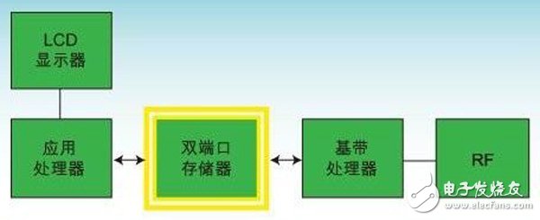
Figure 2: Low-power dual-port devices are ideal for multimedia smartphones
When each FIFO operates independently with its own clock, the shared memory bandwidth between data inputs, control signals, and status flags can become a limiting factor. When a read or write operation is initiated, the sequencer circuit accesses the physical memory in a fast TDM clock domain. It then transfers the data back to the original FIFO clock domain, which introduces latency. This clock domain crossing inherently limits the performance of the FIFO, especially when multiple FIFOs are involved. Some leading FPGA vendors even recommend limiting the number of FIFOs in a design to no more than 10 for high-performance applications.
There are also performance challenges when configuring an FPGA as a dual-port memory. In many cases, FPGAs are used alongside ASICs, and performance is constrained by three key factors: the internal speed of the dual-port memory, the settling time of the ASIC input, and the external speed at which the ASIC can access the dual-port information. These limitations must be carefully considered to ensure optimal system performance.
Hydrogel Film,Film Tpu Flexible Hd,Hydrogel Vs Glass,Tpu Film
Shenzhen TUOLI Electronic Technology Co., Ltd. , https://www.tlhydrogelprotector.com